- 您现在的位置:买卖IC网 > Sheet目录2001 > ISL26329FVZ (Intersil)IC ADC 12BIT SPI/SRL 16-TSSOP
ISL26320, ISL26321, ISL26322, ISL26323, ISL26324, ISL26325, ISL26329
13
FN8273.1
September 5, 2013
Analog Inputs
Some members of the ISL26320, ISL26321, ISL26322,
ISL26323, ISL26324, ISL26325 and ISL26329 family feature a
fully differential input with a nominal full-scale range equal to
twice the applied VREF voltage. Those devices with differential
inputs have a nominal full scale range equal to twice the applied
VREF voltage. Each input swings VREF volts (peak-to-peak), 180°
out of phase from one another for a total differential input of
Differential signaling offers several benefits over a single-ended
input, such as:
Doubling of the full-scale input range (and therefore the
dynamic range)
Improved even order harmonic distortion
Better noise immunity due to common mode rejection
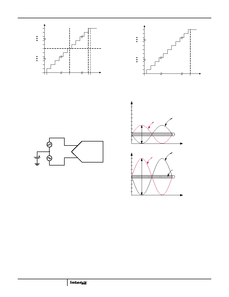
Figure 24 shows the relationship between the reference voltage
and the full-scale differential input range for two different values
of VREF. Note that the common-mode input voltage must be
maintained within ±200mV of VREF/2 for differential inputs.
Those devices with singled-ended inputs have a ground-referenced
peak-to-peak input voltage span equal to the reference voltage.
FIGURE 21. IDEAL TRANSFER CHARACTERISTICS, DIFFERENTIAL INPUT
FIGURE 22. IDEAL TRANSFER CHARACTERISTICS, SINGLE-ENDED INPUT
1LSB = 2VREF/4096
100...000
100...001
100...010
111...111
000...000
000...001
011...110
011...111
AD
C
O
DE
ANALOG INPUT
AIN+ – (AIN–)
–V
REF
+ LSB
+VREF
– 1LSB
0V
+VREF
– 1LSB
1LSB = VREF/4096
000...000
000...001
000...010
011...111
100...000
100...001
111...110
111...111
AD
C
O
DE
ANALOG INPUT
0 = + LSB
FS = +VREF-1LSB
FIGURE 23. DIFFERENTIAL INPUT SIGNALING
ISL2631X/32X
VCM
VREF (P-P)
AIN+
AIN-
FIGURE 24. RELATIONSHIP BETWEEN VREF AND FULL-SCALE
RANGE FOR DIFFERENTIAL INPUTS
3.0
5.0
2.0
1.0
4.0
AIN+
AIN–
2.5Vp-p
VREF = 2.5V
3.0
5.0
2.0
1.0
4.0
AIN+
AIN–
VCM
5Vp-p
VREF = 5V
t
V
t
V
ALLOWABLE VCM RANGE
发布紧急采购,3分钟左右您将得到回复。
相关PDF资料
ISL2671286IBZ
IC ADC 12BIT SPI/SRL 20K 8SOIC
ISL26712IRTZ
IC ADC 12BIT SAR 1MSPS 8-TDFN
ISL267450AIUZ
IC INTERFACE
ISL267817IUZ
IC INTERFACE
ISL32272EIVZ-T
IC TX RS422 QUAD 16TSSOP
ISL32273EIVZ
IC RCVR RS485/422 QD ESD 16TSSOP
ISL32470EIBZ-T7A
IC TXRX RS485 FAULT PROT 14SOIC
ISL32483EIBZ-T7A
IC TXRX RS485 FAULT PROT 14SOIC
相关代理商/技术参数
ISL26329FVZ-T
功能描述:IC ADC 12BIT SPI/SRL 16-TSSOP RoHS:是 类别:集成电路 (IC) >> 数据采集 - 模数转换器 系列:- 产品培训模块:Lead (SnPb) Finish for COTS
Obsolescence Mitigation Program 标准包装:250 系列:- 位数:12 采样率(每秒):1.8M 数据接口:并联 转换器数目:1 功率耗散(最大):1.82W 电压电源:模拟和数字 工作温度:-40°C ~ 85°C 安装类型:表面贴装 封装/外壳:48-LQFP 供应商设备封装:48-LQFP(7x7) 包装:管件 输入数目和类型:2 个单端,单极
ISL26329FVZ-T7A
功能描述:IC ADC 12BIT SPI/SRL 8CH 16TSSOP RoHS:是 类别:集成电路 (IC) >> 数据采集 - 模数转换器 系列:- 产品培训模块:Lead (SnPb) Finish for COTS
Obsolescence Mitigation Program 标准包装:1 系列:- 位数:10 采样率(每秒):357k 数据接口:DSP,MICROWIRE?,QSPI?,串行,SPI? 转换器数目:1 功率耗散(最大):830µW 电压电源:单电源 工作温度:-40°C ~ 85°C 安装类型:表面贴装 封装/外壳:10-WFDFN 裸露焊盘 供应商设备封装:10-TDFN-EP(3x3) 包装:剪切带 (CT) 输入数目和类型:2 个单端,单极;2 个单端,双极;1 个差分,单极;1 个差分,双极 产品目录页面:1396 (CN2011-ZH PDF) 其它名称:MAX1395ETB+TCT
ISL26708
制造商:INTERSIL 制造商全称:Intersil Corporation 功能描述:12-Bit, 10-Bit and 8-Bit, 1MSPS SAR ADCs
ISL26708IHZ-T
功能描述:IC ADC 8BIT SPI/SRL 1M 8-SOT-23 RoHS:是 类别:集成电路 (IC) >> 数据采集 - 模数转换器 系列:- 产品培训模块:Lead (SnPb) Finish for COTS
Obsolescence Mitigation Program 标准包装:250 系列:- 位数:12 采样率(每秒):1.8M 数据接口:并联 转换器数目:1 功率耗散(最大):1.82W 电压电源:模拟和数字 工作温度:-40°C ~ 85°C 安装类型:表面贴装 封装/外壳:48-LQFP 供应商设备封装:48-LQFP(7x7) 包装:管件 输入数目和类型:2 个单端,单极
ISL26708IHZ-T7A
功能描述:IC ADC 8BIT SPI/SRL 1M 8SOT-23 RoHS:是 类别:集成电路 (IC) >> 数据采集 - 模数转换器 系列:- 产品培训模块:Lead (SnPb) Finish for COTS
Obsolescence Mitigation Program 标准包装:1 系列:- 位数:10 采样率(每秒):357k 数据接口:DSP,MICROWIRE?,QSPI?,串行,SPI? 转换器数目:1 功率耗散(最大):830µW 电压电源:单电源 工作温度:-40°C ~ 85°C 安装类型:表面贴装 封装/外壳:10-WFDFN 裸露焊盘 供应商设备封装:10-TDFN-EP(3x3) 包装:剪切带 (CT) 输入数目和类型:2 个单端,单极;2 个单端,双极;1 个差分,单极;1 个差分,双极 产品目录页面:1396 (CN2011-ZH PDF) 其它名称:MAX1395ETB+TCT
ISL26708IRTZ
功能描述:IC ADC 8BIT SAR 1MSPS 8-TDFN RoHS:是 类别:集成电路 (IC) >> 数据采集 - 模数转换器 系列:- 产品培训模块:Lead (SnPb) Finish for COTS
Obsolescence Mitigation Program 标准包装:250 系列:- 位数:12 采样率(每秒):1.8M 数据接口:并联 转换器数目:1 功率耗散(最大):1.82W 电压电源:模拟和数字 工作温度:-40°C ~ 85°C 安装类型:表面贴装 封装/外壳:48-LQFP 供应商设备封装:48-LQFP(7x7) 包装:管件 输入数目和类型:2 个单端,单极
ISL26708IRTZ-T
功能描述:IC ADC 8BIT SAR 1MSPS 8-TDFN RoHS:是 类别:集成电路 (IC) >> 数据采集 - 模数转换器 系列:- 产品培训模块:Lead (SnPb) Finish for COTS
Obsolescence Mitigation Program 标准包装:250 系列:- 位数:12 采样率(每秒):1.8M 数据接口:并联 转换器数目:1 功率耗散(最大):1.82W 电压电源:模拟和数字 工作温度:-40°C ~ 85°C 安装类型:表面贴装 封装/外壳:48-LQFP 供应商设备封装:48-LQFP(7x7) 包装:管件 输入数目和类型:2 个单端,单极
ISL26708IRTZ-T7A
功能描述:模数转换器 - ADC 08 BIT 1MSPS SAR ADC RoHS:否 制造商:Texas Instruments 通道数量:2 结构:Sigma-Delta 转换速率:125 SPs to 8 KSPs 分辨率:24 bit 输入类型:Differential 信噪比:107 dB 接口类型:SPI 工作电源电压:1.7 V to 3.6 V, 2.7 V to 5.25 V 最大工作温度:+ 85 C 安装风格:SMD/SMT 封装 / 箱体:VQFN-32